Manufacturer Custom High Purity P Type Dopant Single Side Polished Silicon Wafer
Manufacturer Custom High Purity P Type Dopant Single Side Polished Silicon Wafer
Item Number:X-P24Z2L1202
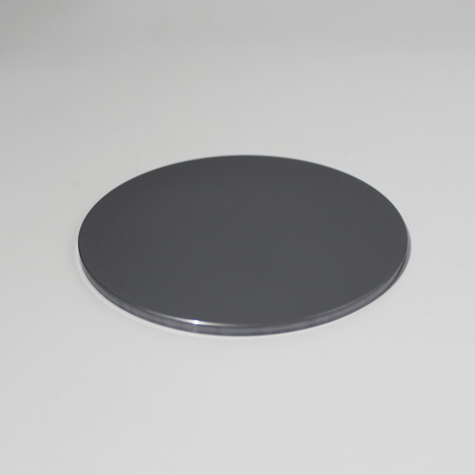
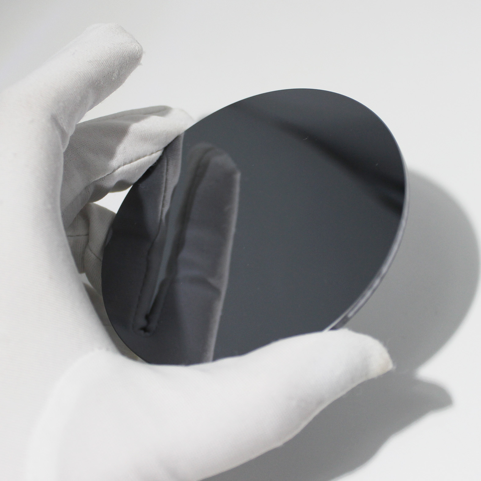
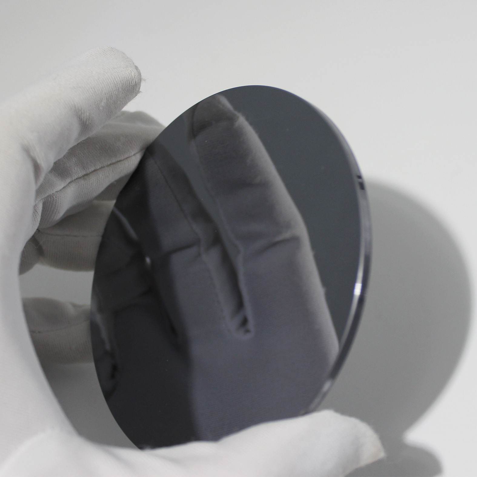
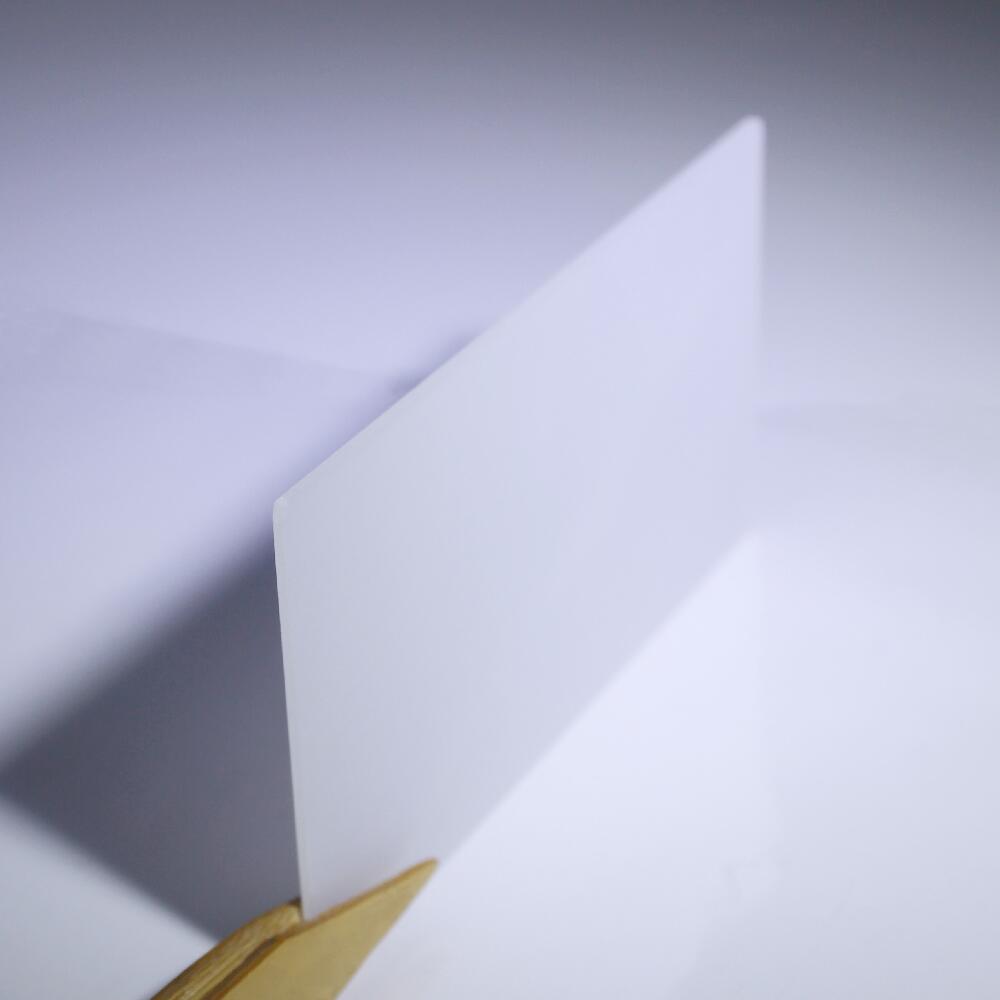
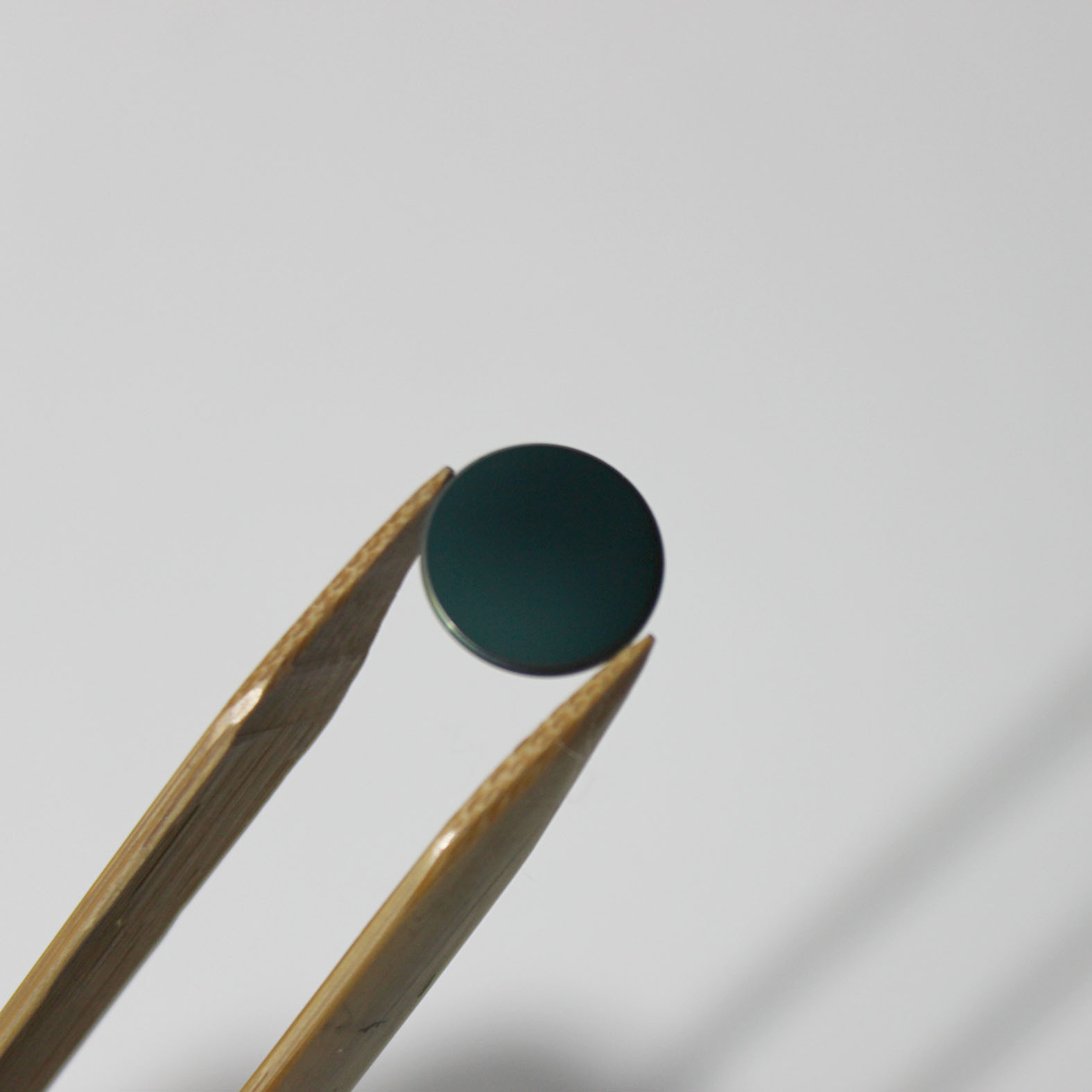
A silicon wafer is a material essential for manufacturing semiconductors, which are found in all kinds of electronic devices that enrich our lives.Few of us have a chance to encounter an actual silicon wafer in daily life. This ultra-flat disk is polished to a mirror-like surface, and made as free as possible of tiny surface irregularities, making it the flattest object in the world. It is also ultra-clean, virtually free of microparticles and other impurities. These qualities are necessary so it can be used as the substrate material of today's state-of-the-art semiconductors.
- Material: Silicon
- Dimension: Dia. 45.00mm
- Thickness: 2.00mm
- Tolerance : +/-0.10mm
What is Silicon Wafer?
Silicon wafer is a material used for producing semiconductors, which can be found in all types of electronic devices that improve the lives of people. Silicon comes second as the most common element in the universe; it is mostly used as a semiconductor in the technology and electronic sector.
Most people have had the chance to encounter a real silicon wafer in their life. This super-flat disk is refined to a mirror-like surface. Besides, it is also made of subtle surface irregularities which make it the flattest object worldwide.
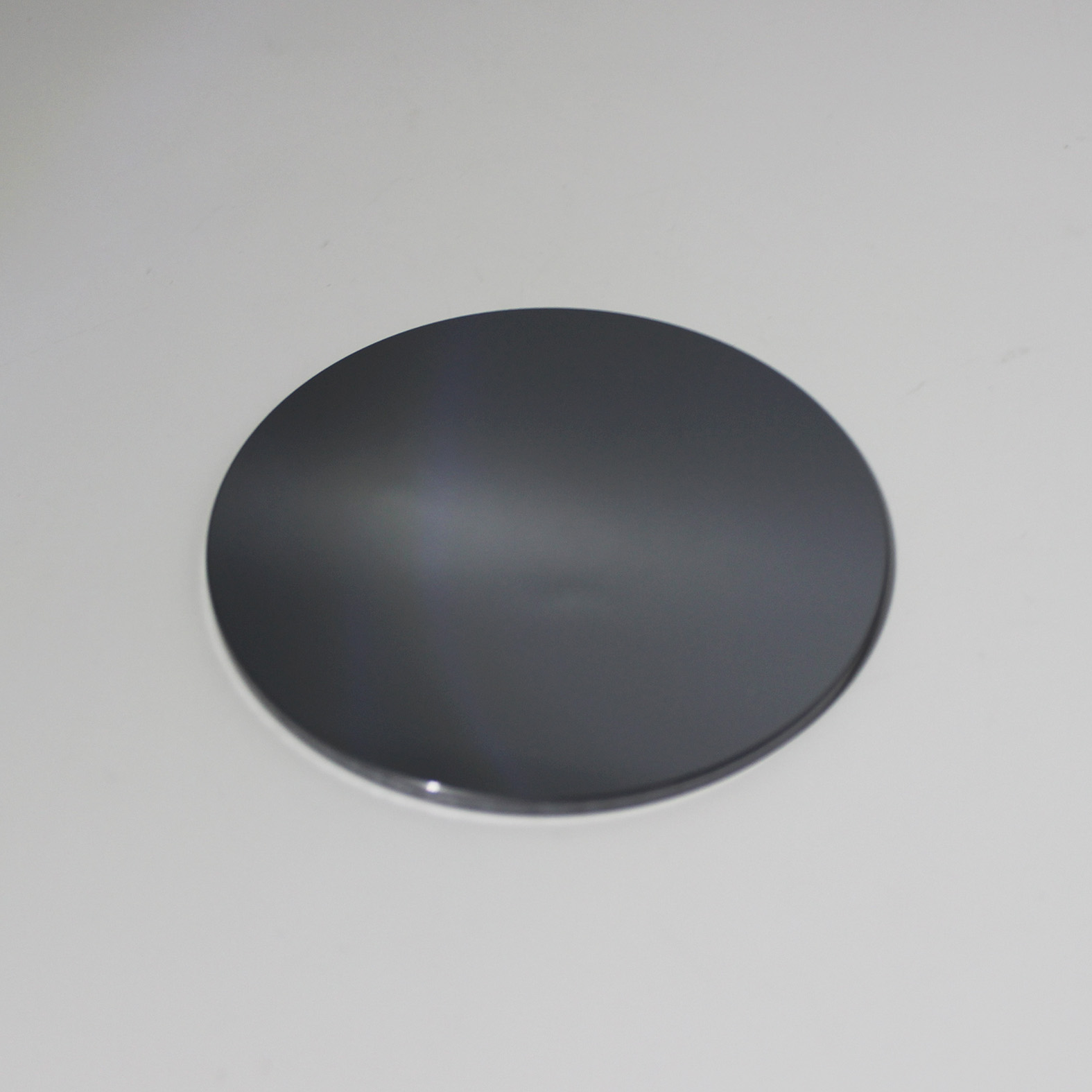
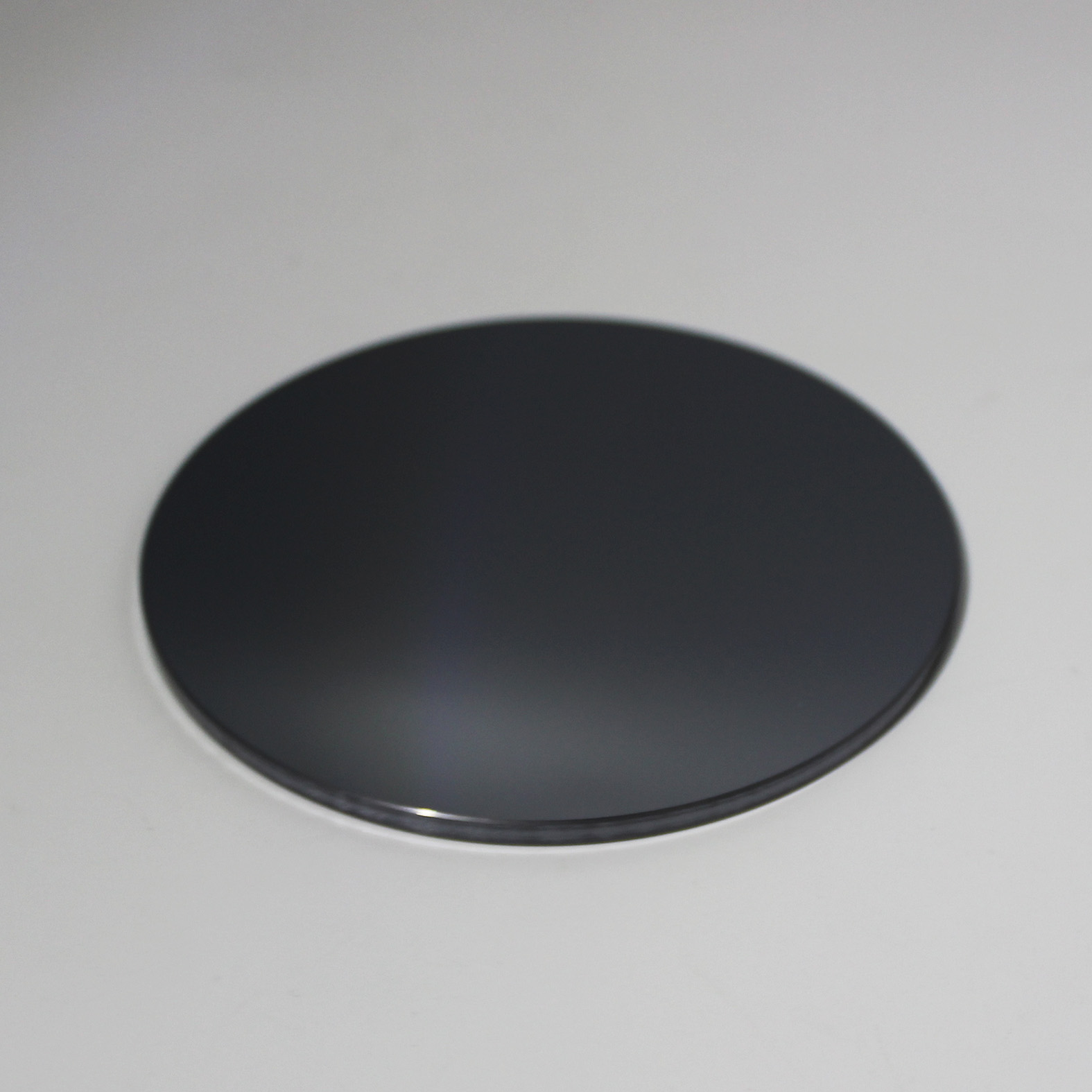
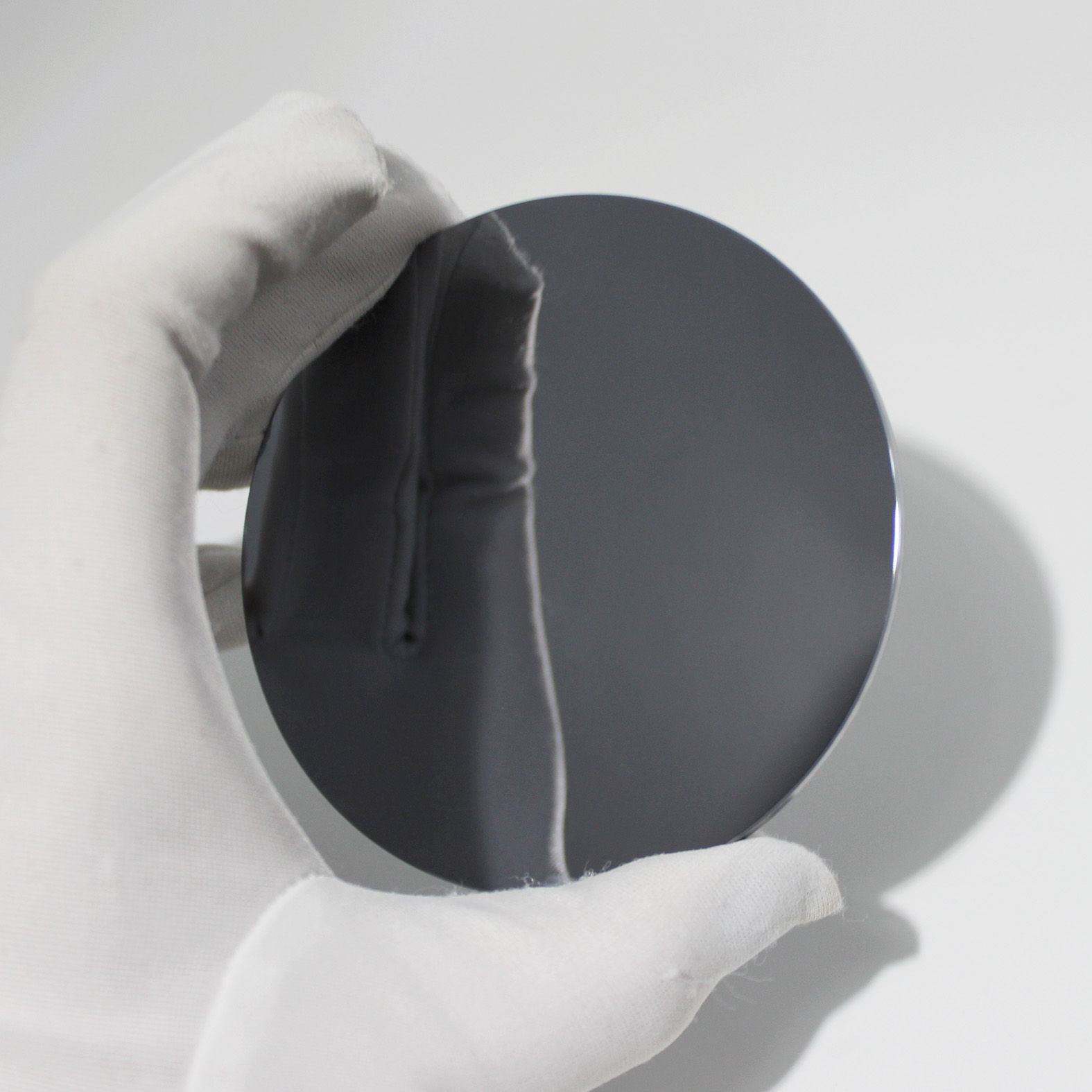
Picture of Polished Silicon Wafer

Specifications of High Purity Si Wafer
| Specification | Data |
| Diameter | 85mm |
| Thickness | 3mm |
| Growth Method | CZ |
| Orientation | <100> |
| P Type Dopant | Typtical Boron |
| Resistivity | 0.001~0.005Ω |
| TTV | <10um |
| Polished Surface | Single Side |
Video of 85mm Silicon Wafer
What Is The Silicon Wafer Used For?
1. Semiconductor
Even though other conductors are employed in more particular applications, silicon is the best and the most used semiconductor due to its extreme mobility both at high temperatures and at room temperature.
What makes Silicon an outstanding option in electronic devices is because its electrical currents can pass via the silicon conductors much quicker compared to other conductors.
2. Silicon Wafers In Electronic Devices
Semiconductors such as the silicon wafer can be used in the production of both chips and microchips in electronic gadgets.
Due to the uniqueness of the electrical currents via silicon wafers, these semiconductors are used in creating ICs (integrated circuits). The ICs act as commands for specific actions in various electronic devices.
The Silicon wafer is the main element in integrated circuits. Simply put, integrated circuits are a composite of a variety of electronic elements that are brought together to perform a particular function.
Silicon is the key platform for semiconductor gadgets. A wafer is just but a thin slice of the semiconductor material that acts as a substratum for microelectronic devices fitted in and above the wafer.
Even if it can be simple to relate silicon wafers with very particular technological devices that individuals only dream of, silicon wafers are way much closer than anyone may think!
Silicon wafers are used in computers, smartphones, and mobile devices and even in the tire pressure sensor system.
Manufacturing of the silicon wafer is an incredibly vital part of the establishment and expansion of a broad range of technological advancements.
3. Other Uses of Silicon Wafers
The ultra-pure silicon wafers offer a pristine canvas on which to fabricate the integrated circuitry central to all electronics. The uses include:
Microprocessors - The central chips powering computers and smartphones
DRAM & flash memory - Billions of silicon-based memory cells on chips
CMOS sensors - Image sensors capturing light in smartphone cameras and more
Power devices - Specialized designs managing electricity in systems
MEMS - Tiny mechanical and electromechanical silicon systems
Optical circuits - Waveguides and photonic devices integrate optics
Want to learn more / get a quote? Just click here to contact us now~ 
Related Products
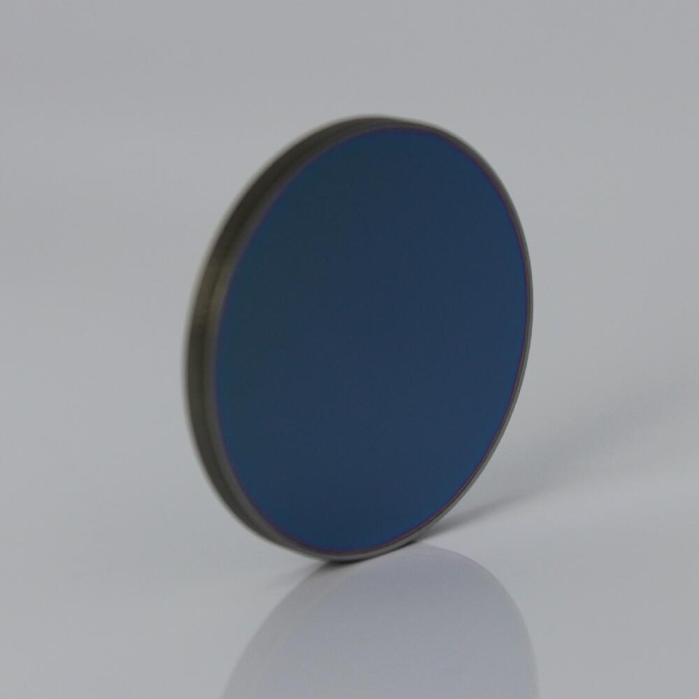
China Optical High Quality Germanium Windows/Wafer with AR Coating
Germanium is an optical material completely impervious to ultraviolet and visible light, ...
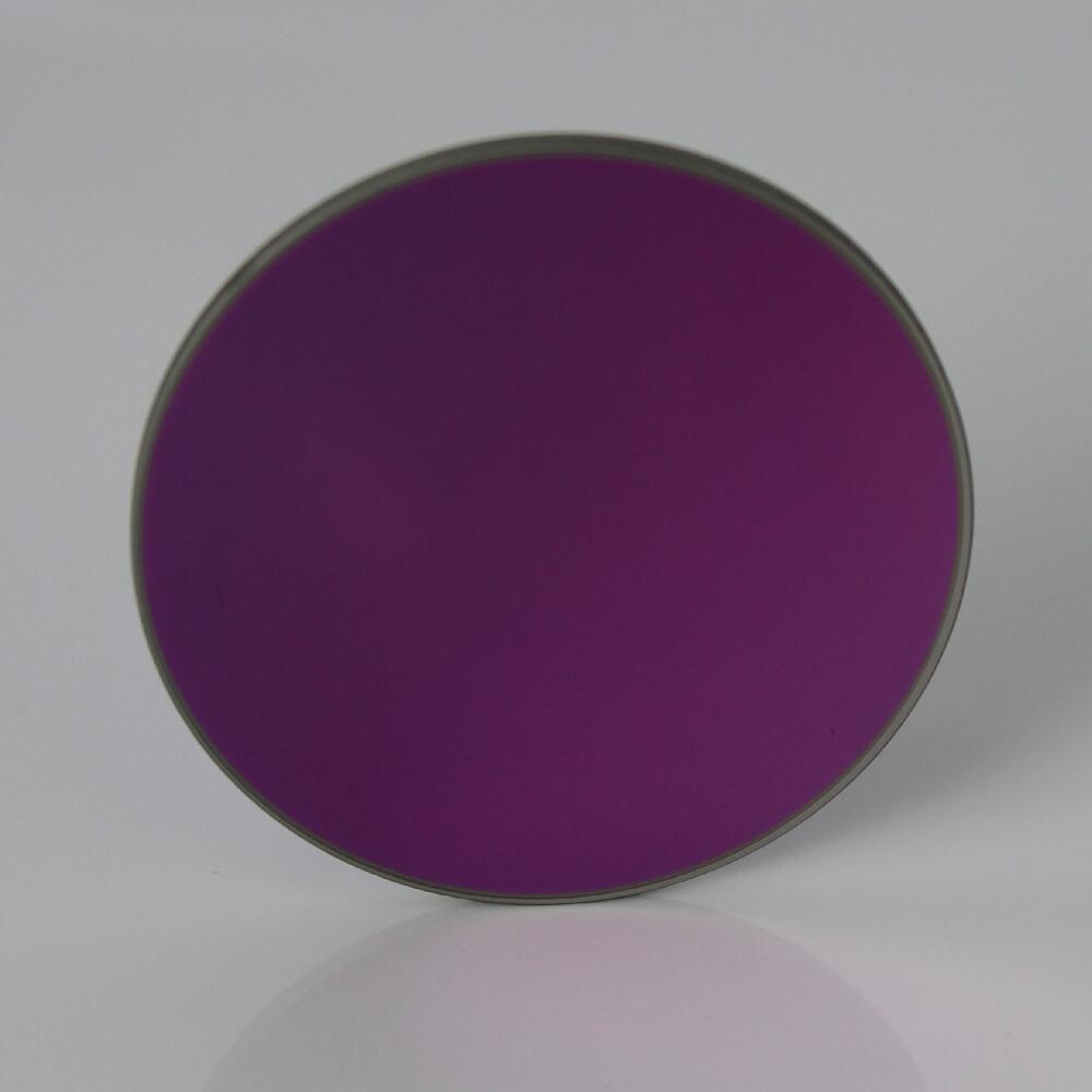
High Quality AR Coated Optical Germanium Crystal Wafer for Semiconductor From China
Germanium is an optical material completely impervious to ultraviolet and visible light, ...
Customized High Quality Optical LiNbO3 wafer LT Window in Stock from China
Lithium Niobate (LiNbO3) is a well-developed crystalline material characterized by a high ...
Hot Selling Custom Polishing Surface AR Coating Germanium Wafer
Germanium is an optical material completely impervious to ultraviolet and visible light, ...