Lithium niobium (LiNbO3) crystal

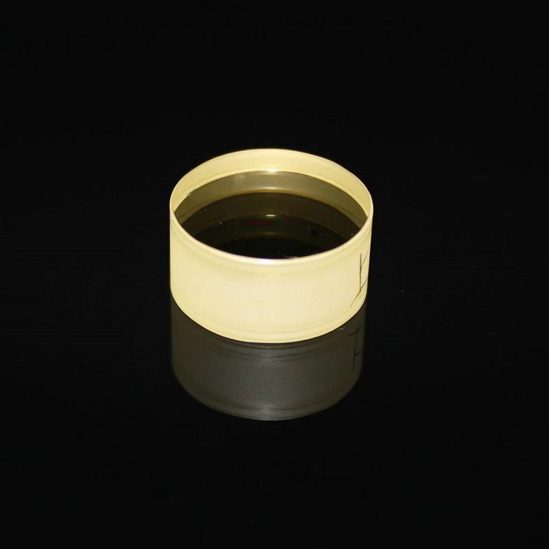
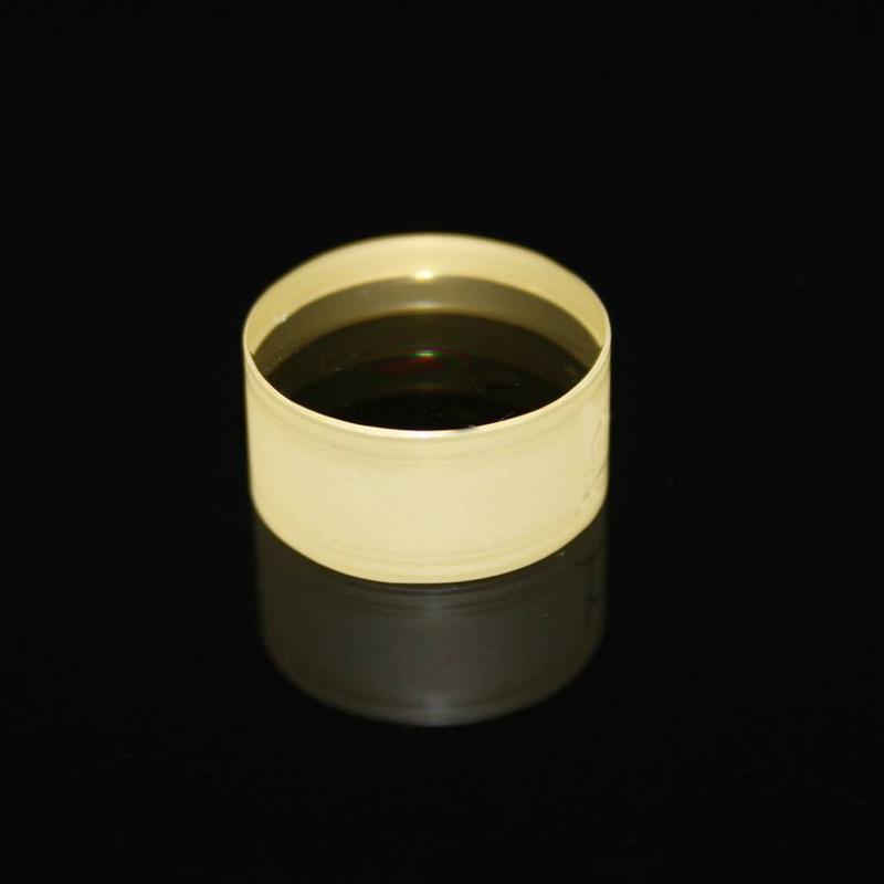
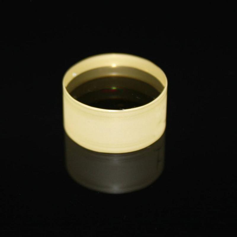
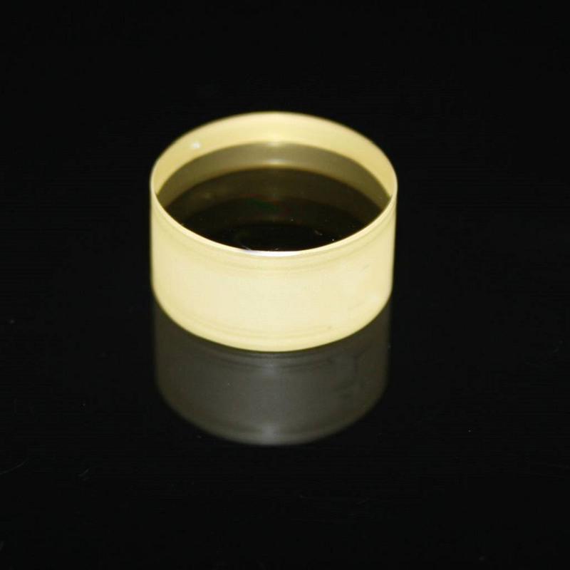
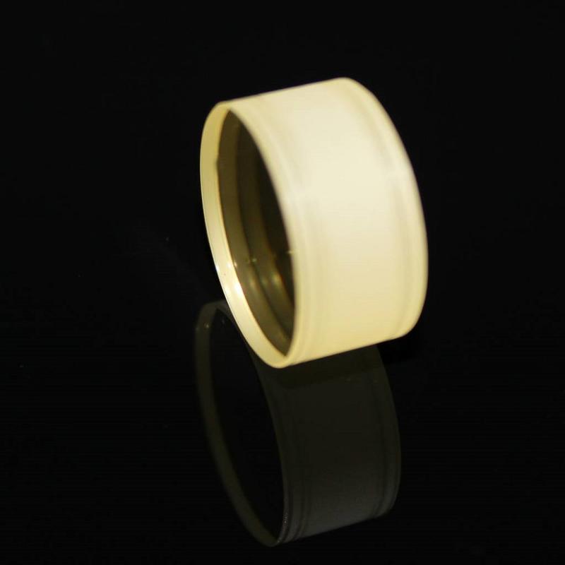
Lithium niobium (LiNbO3) crystal
Item Number:W-D20T10A
- Material: LT, LN etc..
- Dimension: 5mm-460mm
- Thickness: 0.1mm-30mm
- Surface Accuracy: lambda/8
- Surface Quality: 20/10
- Tolerance: +/-0.01mm
- Parallelism: 30"
About Lithium niobium (LiNbO3) wafer
Lithium niobium crystal (LN)LiNbO3 lens is widely used in SAW filter, optical waveguide, photoelectricity modulator, frequency multiplication transducer and information storage as a functional crystal with excellent physical feature of anti high temperature and anti canker. It has stable mechanical performance, and will appear different special feature after being doped differently.
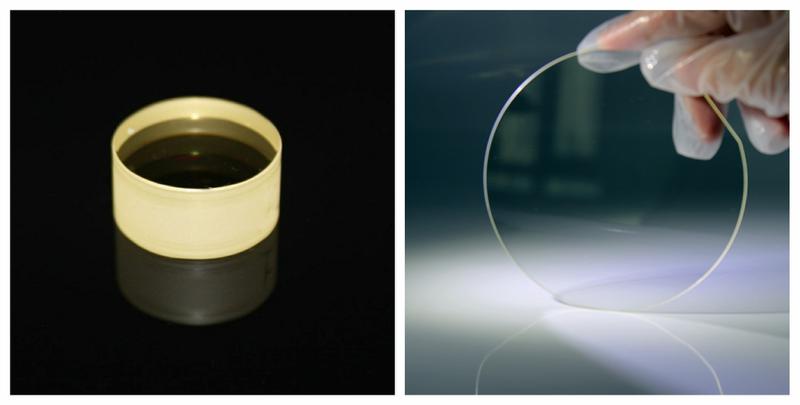
(Picture show of our Lithium niobium)
1. Saw Grade LiNbO3(LN)
● Typical Specifications
| Cutting Angle | Deg. | X/Y/Z/Y36/Y42/Y48/X112 etc | |
| Diameter/size | mm | 3”/76.2 | 4”/100 |
| Tol(±) | mm | 0.25 | 0.5 |
| Thickness | mm | 0.10mm or more | 0.18mm or more |
| Primary reference flat | mm | 22mm or customized | 32.5mm or customized |
| LTV (5mmx5mm) | µm | < 2 | < 2 |
| TTV | µm | < 8 | < 10 |
| Bow | µm | ±20 | ±25 |
| Warp | % | ≤ 30 | ≤ 40 |
| PLTV | ≥95%(5mm*5mm) | ≥95%(5mm*5mm) | |
| Orientation Flat | All available | ||
| Surface Type | Single Side Polished /Double Sides Polished | ||
| Polished side Ra | nm | ≤1 | |
| Back Side Criteria | µm | General is 0.2-0.5 or as customized | |
| Edge Rounding | mm | Compliant with SEMI M1.2 Standard/refer to IEC62276 | |
● Basic materials characteristics
| Crystal symmetry | Trigonal, 3m |
| Lattice constant, A | a = 5.154 c = 13.783 |
| Density, g/cm3 | 7.45 |
| Melting point , °C | 1650 |
| Curie point , °C | 605 |
| Mohs hardness | 6 |
| Thermal expansion coefficient, 10-6/ °C | aa = 16 ac = 4 |
| Thermal conductivity , mW/cm °C | 46 |
| Dielectric Constant (@ 100 KHz) | ea = 54 ec = 43 |
| Refractive indices @ 633 nm | no = 2.175 ne = 2.180 |
| Pyroelectric Coefficient | -2.3 10-4 C/°C/m2 |
● The possible applications
1) Lithium niobate is used extensively in the telecoms market:
a) in mobile telephones and optical modulators. It is the material of choice for the manufacture of surface acoustic wave devices.
b) in laser frequency doubling, nonlinear optics, Pockels cells, optical parametric oscillators, Q-switching devices for lasers, other acousto-optic devices, optical switches for gigahertz frequencies
c) It is an excellent material for manufacture of optical waveguides.
2) It's also used in the making of optical spatial low-pass (anti-aliasing) filters.
2. Optical Grade LN Wafer
● Typical Specifications
| Orientation | X&Z-cut ±0.2° |
| Diameter | 50.8mm/76.2 mm/100mm ±0.3 mm |
| Orientation Flat(OF) | 22mm ±2 mm/32mm ±2 mm Perpendicular to X ±0.2° |
| Second Refer.Flat(RF) | Cw225°±0.5°from OF Cw315°±0.5°from OF |
| Thickness | 250um/500um/1000um ±5um or more |
| Surface Quality | Double sides polished; S/D:20/10 |
| TTV | ≤10um |
| WARP | ≤50um |
| Curie Temperature | 1142℃± 0.7℃ |
| Refractive Index | n。=2.2878±0.0002 n。=2.2033±0.0002 prism coupler method@632.8nm |
| Edge Beveling | Edge Rounding |
Customization acceptable
● Basic materials characteristics
| Crystal Structure | Trigonal, point group 3m |
| Lattice Parameters | a=5.148Å, c=13.863Å |
| Density | 4.64 g/cm3 |
| Melting Point | 1250 °C |
| Curie Point | 1142±2℃ |
| Mohs Hardness | 5 |
| Dielectric Constant | e11/e0 = 85; e33/e0 = 29.5 |
| Thermal Conductitiy | 38 W/m/°C at 25°C |
| Thermal Expansion Coefficient | a1=a2 =2x10⁻⁶/°C, a3=2.2x10⁻⁶/ °C at 25°C |
| Elastic Stiffness Constant | CE11 = 2.04 x 10¹¹ N/m2, CE33 = 2.46 x 10¹¹ N/m2 |
● The possible applications
1) EO Waveguide Phase Modulators
2) EO Waveguide Amplitude Modulators
3) Integrated Waveguide Photonics
4) Wave Guide Lasers