Innovative design of optical system
Optical, mechanical designs
The design of high-end optical systems for a demanding application usually starts with the specification of the six main parameters: magnification, focal distance, resolution, depth of focus, spectral range, and target customer price.
The magnification (m, which describes the optical magnification of the physical image onto the image sensor) of an optical system should be aligned with the resolution of the image and therefore the pixel size of the employed image sensor to form the small print of interest visible. together with the front focal distance (fo) of the optical system (given by a working distance for a selected application), the rear focal distance (fi, the space from the last camera lens to the image sensor) is often calculated as fi = m × fo.
The resolution and depth of focus of an optical system are influenced by the focal ratio (F#). The F# is additionally a crucial factor for image brightness (depending on the image sensor sensitivity) and is defined as F# = f/D, where f is that the focal distance of the optical system and D is that the optical diameter. it's possible to realize higher resolution with a bigger F#, but at an equivalent time the depth of focus (DoF) — the acceptance range for focus variations while still having a pointy image — becomes shorter. Especially in industrial metrology applications, a high DoF is desirable, because it reduces the necessity for refocusing. Resolution and DoF, therefore, got to be balanced during the planning phase, whereby both enjoy bright images and good illumination conditions. As a result of diffraction, the resolution of an optical system reaches a fundamental maximum. An optical system with the power to supply images at a resolution nearly as good because the instrument’s theoretical limit is claimed to be diffraction limited.
The spectral range of the optical application describes rock bottom and the highest required optical wavelengths for the precise application. It strongly influences the sort of glass used for optical elements (lenses, prisms, filters, etc.) and may significantly complicate the general optical design. From a design point of view, low-dispersion glasses are most favorable for optical elements, since they require little effort to catch up on aberration but often accompany short spectral ranges and high prices. As a result, the worth of an optical system is strongly influenced not only by the specified resolution and magnification within the optical application but also by the specified spectral range, which drives the fabric cost of optical elements.
Tolerating an objective lens
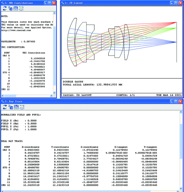
Once the nominal optical design is fixed and every one theoretical system parameters are achieved, the optical designer performs a so-called tolerance analysis. This procedure allows the designer to tolerate the optical elements in terms of acceptable alignment accuracies (including what's needed for mechanical mounts), also because of the manufacturing tolerances for all-optical elements, like center thickness variation, glass homogeneity, and surface irregularities. for instance, demanding metrology applications like interferometers require objective lens designs with minimal tolerances to realize valid measurement results.
During the mechanical design phase, all alignment accuracies and application requirements are taken under consideration and wont to build a mechanical model with classical CAD software. Here, special mounting techniques for low-stress interfaces of optical and mechanical parts are of high importance for diffraction-limited optical systems.
In particular, many semiconductor applications require special gluing. Designs with large optical elements often involve special mounting strategies and flexure hinges to make sure performance in variable-temperature environments. Also, the selection of fabric for mechanical parts comes into play when long-term stability and enormous working temperature ranges are required. In some cases, mixtures of varied mechanical materials with different thermal expansion coefficients are wont to achieve athermal behavior. Here, choosing the proper mounting technology (gluing, bonding, mechanical fixtures, etc.) requires extensive design experience and a deep understanding of the customer application.
Optical element accuracy
After the mechanical design is finalized, which frequently includes tolerancing loops with the lead optical designer, the assembly of optical and mechanical parts are often started.
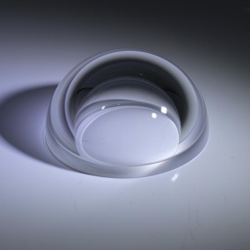
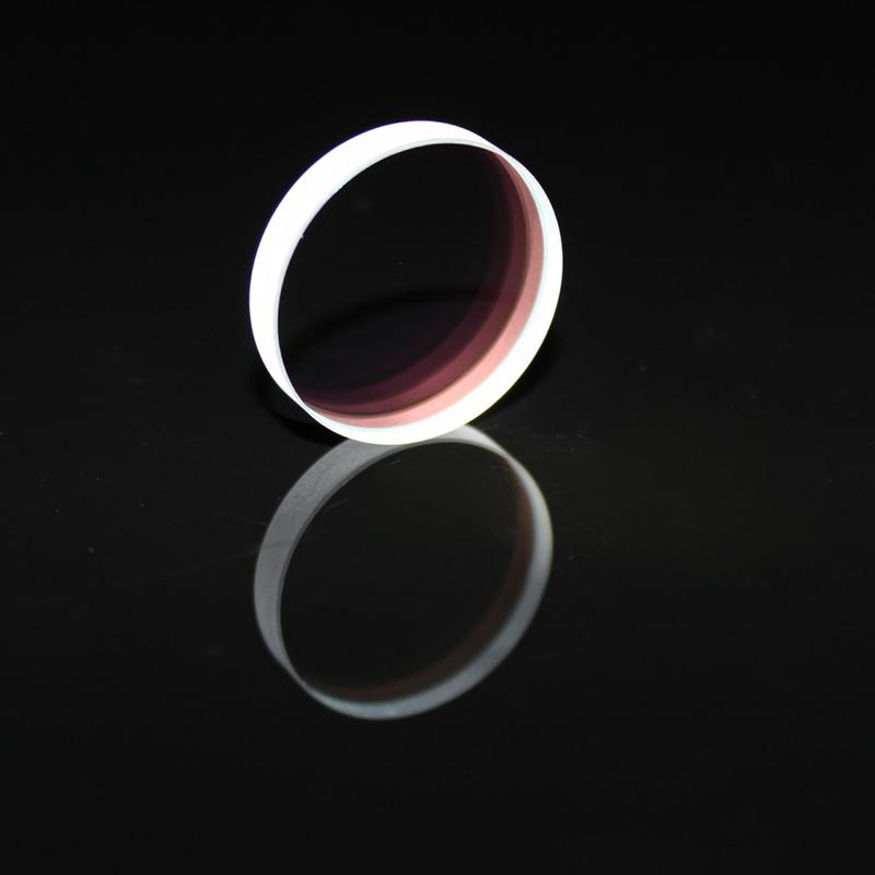
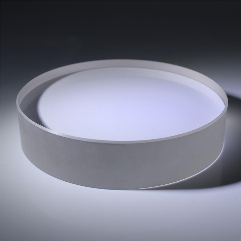
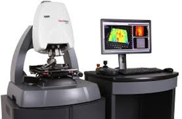
The required optical elements are derived from a pure block of glass, first by grinding then by polishing the glass surface. counting on the manufacturing process, high-precision optical elements require fine correction steps after polishing, which involves technologies like ionic beam finishing, magnetorheological finishing, or fine polishing or etching with specialized tools. However, today the accuracy of the top product isn't limited by the machining tools, but by the accuracy of the metrology equipment. Surface irregularities of a couple of nanometers for optical elements with diameters of fifty to 500 mm are typical for optics utilized in semiconductor metrology applications.
In modern cleanroom metrology areas with temperature-stabilized conditions, it's possible to live form variations below 1 nm on the whole optical surface and proper for it during a closed-loop manner. for several applications — including machine vision, medical devices, and optical microscopy — these accuracies are sufficient, but semiconductor applications always push for brand spanking new limits. Even today, with modern fabrication technologies and metrology equipment, only a couple of companies worldwide can manufacture optical elements with high-precision requirements out of demanding glass materials. Designing and manufacturing optical systems at the sting of what's technically possible are some things that needs decades of experience.
Optomechanical assembly
When all optical components are manufactured, inspected, and coated, and every one mechanical parts are finished, the optomechanical assembly are often started. Ideally, the mechanical design has been performed, such only short assembly steps are required and straightforward integration of tilt- and decentration-sensitive optical elements are often semi- or fully automated.
For diffraction-limited optical systems, the assembly often involves manual work and in place metrology, using compensation strategies to realize a wonderfully aligned optical system. In many cases, specialized assembly and metrology setups must be developed to permit assembly, iterative use of metrology, and functional testing at or on the brink of the environmental working conditions of the ultimate application.
Lenses designed and made for high-resolution and diffraction-limited performance under harsh environmental conditions require a seriously planned final quality check, also as quality tests for its subassemblies, checking for well-centered lenses with low tolerances on tilt, decentration, center thickness, and precise interns distances. For diffraction-limited performance, optical compensators are sometimes inevitably adjusted within the micron and even submicron range during final assembly to satisfy all of those requirements.
Correct treatment, neat handling, proper storage, and careful cleaning of optical and mechanical parts throughout the whole production process, especially for the DUV domain, is a must. And assembly in special cleanrooms may be a necessity.
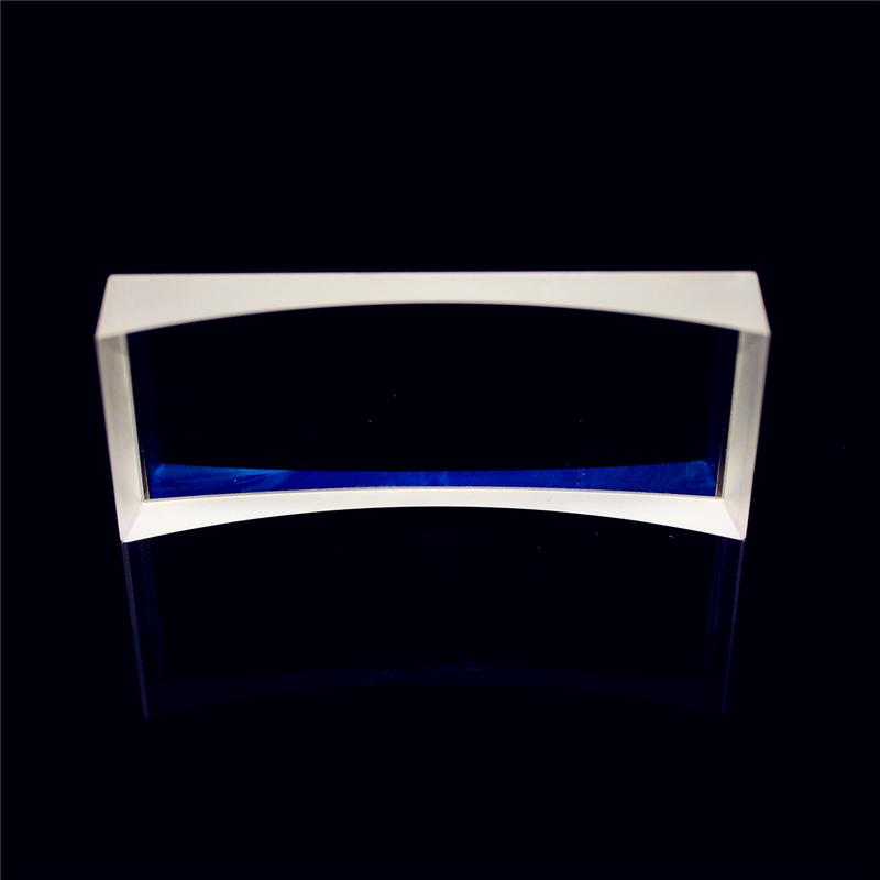
For multispectral or high-resolution applications, beamsplitter prisms inherit play to make the increasing spectrum for multichip sensors or to use superresolution technologies. Sensors should be mounted very precisely within the order of 0.3 μm and must remain stable over temperature drifts and time. this suggests employing a very precise measurement technology together with a stable assembly technology that has special adhesives or new mounting technologies for prisms and sensors. Completing the system with electronics and image sensors consistent with the requirements of the ultimate applications and therefore the demands of the respective customer is another step in generating customized optical systems. Once this is often done, the assemblies are able to be shipped and used, for instance, in 3D scanners as lenses for specific machine vision applications or as measurement devices in other industrial metrology applications.
While many of today’s imaging applications are often addressed with standard optics, the overall increase in image-based metrology systems within the industry is additionally driving the demand for diffraction-limited optical systems. With an outsized sort of applications increasing demands on resolution, sensitivity, and spectral range, the optics’ performance levels still rise. The result: new limits for surface accuracy of optical elements, mechanical design, and assembly technologies.