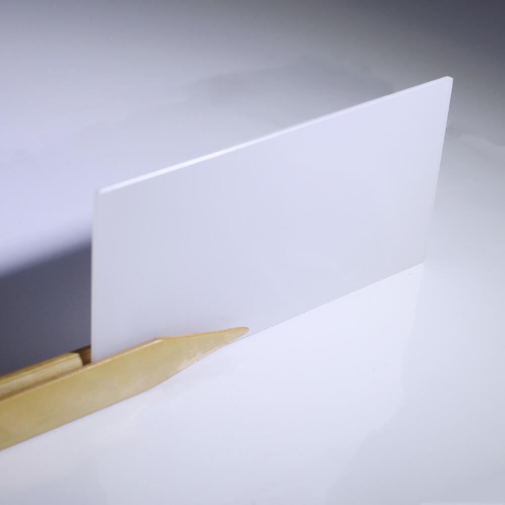
China Manufacture Single-Crystal Products Optical LiNbO3 Crystal Wafers


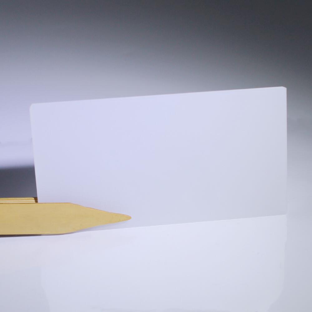
China Manufacture Single-Crystal Products Optical LiNbO3 Crystal Wafers
Item No: X-P22L1T14701
Lithium Niobate (LiNbO3) is a well-developed crystalline material characterized by a high electromechanical coupling coefficient, a wide range of transparency, and excellent chemical and mechanical stability.Single side polishing/double side polishing are all available, cutting angle X/Y/Z etc.They can be used in a wide range of applications including telecommunications and sensing, surface acoustic devices, integrated optics, and novel wavelength generating and refracting elements.VY Optoelectronics Co.,Ltd. can customize various grades and sizes of LiNbO3 wafers according to your requirements.
- Material: LT, LN etc..
- Dimension: 76.20mm
- Thickness: 0.50mm
- Surface Accuracy: lambda/8
- Surface Quality: 20/10
- Tolerance: +/-0.01mm
- Parallelism: 30″
Quote Now
Lithium niobium crystal (LN)LiNbO3 lens is widely used in SAW filter, optical waveguide, photoelectricity modulator, frequency multiplication transducer and information storage as a functional crystal with excellent physical feature of anti high temperature and anti canker. It has stable mechanical performance, and will appear different special feature after being doped differently.
1. Saw Grade LiNbO3(LN)
● Typical Specifications
| Cutting Angle | Deg. | X/Y/Z/Y36/Y42/Y48/X112 etc | |
| Diameter/size | mm | 3”/76.2 | 4”/100 |
| Tol(±) | mm | 0.25 | 0.5 |
| Thickness | mm | 0.10mm or more | 0.18mm or more |
| Primary reference flat | mm | 22mm or customized | 32.5mm or customized |
| LTV (5mmx5mm) | µm | < 2 | < 2 |
| TTV | µm | < 8 | < 10 |
| Bow | µm | ±20 | ±25 |
| Warp | % | ≤ 30 | ≤ 40 |
| PLTV | ≥95%(5mm*5mm) | ≥95%(5mm*5mm) | |
| Orientation Flat | All available | ||
| Surface Type | Single Side Polished /Double Sides Polished | ||
| Polished side Ra | nm | ≤1 | |
| Back Side Criteria | µm | General is 0.2-0.5 or as customized | |
| Edge Rounding | mm | Compliant with SEMI M1.2 Standard/refer to IEC62276 | |
● Basic materials characteristics
| Crystal symmetry | Trigonal, 3m |
| Lattice constant, A | a = 5.154 c = 13.783 |
| Density, g/cm3 | 7.45 |
| Melting point , °C | 1650 |
| Curie point , °C | 605 |
| Mohs hardness | 6 |
| Thermal expansion coefficient, 10-6/ °C | aa = 16 ac = 4 |
| Thermal conductivity , mW/cm °C | 46 |
| Dielectric Constant (@ 100 KHz) | ea = 54 ec = 43 |
| Refractive indices @ 633 nm | no = 2.175 ne = 2.180 |
| Pyroelectric Coefficient | -2.3 10-4 C/°C/m2 |
● The possible applications
1) Lithium niobate is used extensively in the telecoms market:
a) in mobile telephones and optical modulators. It is the material of choice for the manufacture of surface acoustic wave devices.
b) in laser frequency doubling, nonlinear optics, Pockels cells, optical parametric oscillators, Q-switching devices for lasers, other acousto-optic devices, optical switches for gigahertz frequencies
c) It is an excellent material for manufacture of optical waveguides.
2) It’s also used in the making of optical spatial low-pass (anti-aliasing) filters.
2. Optical Grade LN Wafer
● Typical Specifications
| Orientation | X&Z-cut ±0.2° |
| Diameter | 50.8mm/76.2 mm/100mm ±0.3 mm |
| Orientation Flat(OF) | 22mm ±2 mm/32mm ±2 mm Perpendicular to X ±0.2° |
| Second Refer.Flat(RF) | Cw225°±0.5°from OF Cw315°±0.5°from OF |
| Thickness | 250um/500um/1000um ±5um or more |
| Surface Quality | Double sides polished; S/D:20/10 |
| TTV | ≤10um |
| WARP | ≤50um |
| Curie Temperature | 1142℃± 0.7℃ |
| Refractive Index | n。=2.2878±0.0002 n。=2.2033±0.0002 prism coupler method@632.8nm |
| Edge Beveling | Edge Rounding |
Customization acceptable
● Basic materials characteristics
| Crystal Structure | Trigonal, point group 3m |
| Lattice Parameters | a=5.148Å, c=13.863Å |
| Density | 4.64 g/cm3 |
| Melting Point | 1250 °C |
| Curie Point | 1142±2℃ |
| Mohs Hardness | 5 |
| Dielectric Constant | e11/e0 = 85; e33/e0 = 29.5 |
| Thermal Conductitiy | 38 W/m/°C at 25°C |
| Thermal Expansion Coefficient | a1=a2 =2×10⁻⁶/°C, a3=2.2×10⁻⁶/ °C at 25°C |
| Elastic Stiffness Constant | CE11 = 2.04 x 10¹¹ N/m2, CE33 = 2.46 x 10¹¹ N/m2 |
● The possible applications
1) EO Waveguide Phase Modulators
2) EO Waveguide Amplitude Modulators
3) Integrated Waveguide Photonics
4) Wave Guide Lasers
The detailed video of LiNbO3 wafer is as follows:


ANYTHING YOU COULDN’T FIND?
Talk With Our Sales
Vyoptics dedicated to being the supplier you choose for your custom optic fabrication. From volume production to prototype, we will meet any require specifications at the most cost effective solution.
- Free quotes and design consultations
- Comprehensive brochure you can download
- Worry-free returns
- Lightning Delivery
- OEM&ODM
- Fast Respond Or enthusiasm
- Rapid Production
- Low MQQ
SEND US AN EMAIL
Contact Us
Welcome to discuss your purchasing requirements with our customer service.