
High Precision Lithium Niobate LiNbO3 Crystal Wafer for Electro Optical Photonic and Telecommunication Applications

High Precision Lithium Niobate LiNbO3 Crystal Wafer for Electro Optical Photonic and Telecommunication Applications

Item No: X-P20L1X4601

High quality LiNbO3 wafers manufactured from precision lithium niobate crystals for excellent electro optical, piezoelectric, and nonlinear optical performance. These crystal wafers are widely used in optical modulators, waveguides, laser systems, SAW devices, telecommunications, and photonic applications. Custom orientations, dimensions, and surface polishing are available.

Material: LiNbO3
Diameter: 76.2 mm
Thickness: 0.500 mm

Quote Now

    Contact Info

    Additional Information

    What is a LiNbO3 Wafer?

    A LiNbO3 wafer is a crystal substrate manufactured from lithium niobate material.
    It is widely used in electro optical, piezoelectric, and nonlinear optical applications because of its excellent optical and electrical properties.

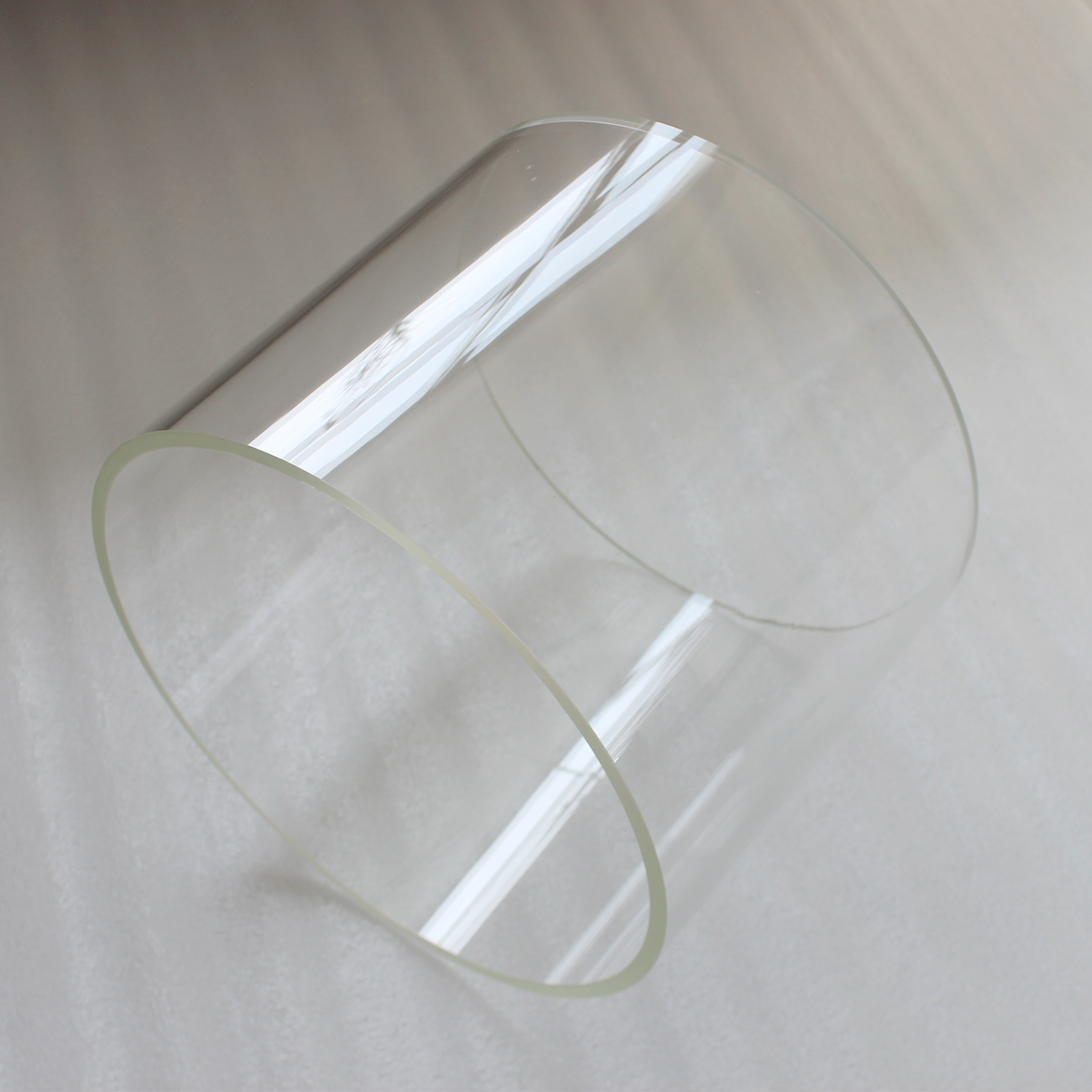
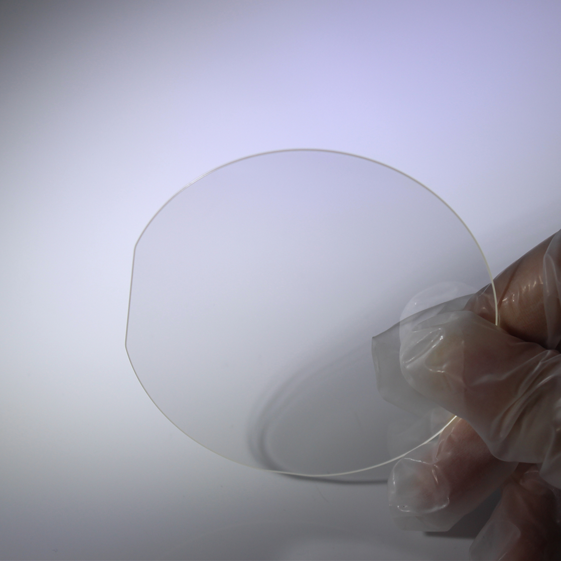
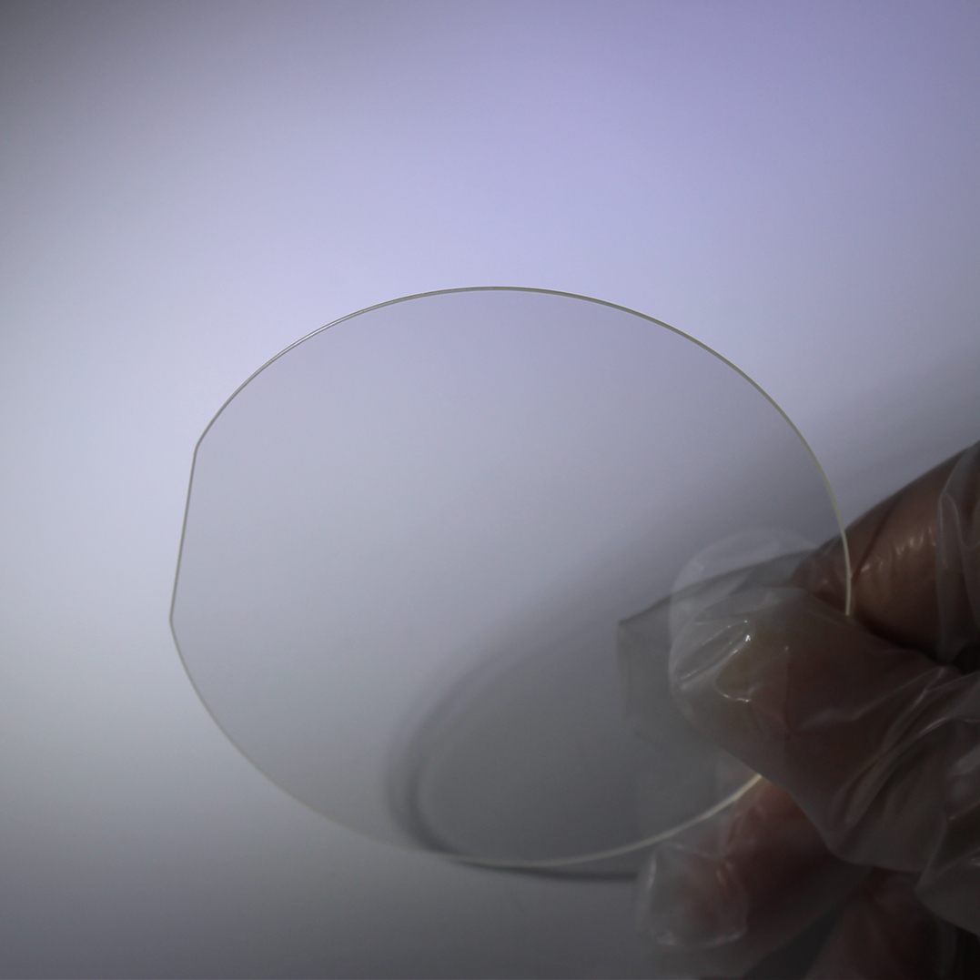
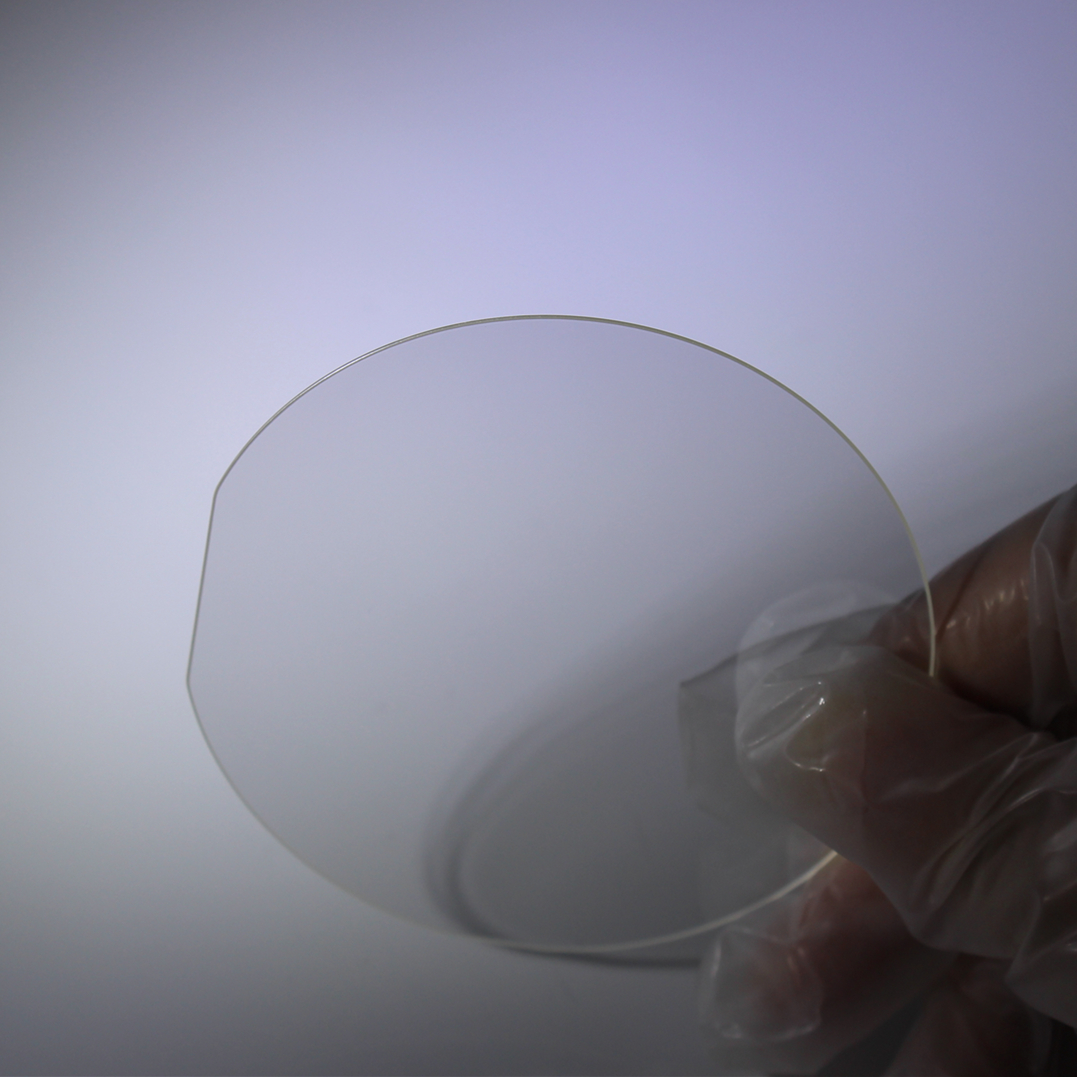
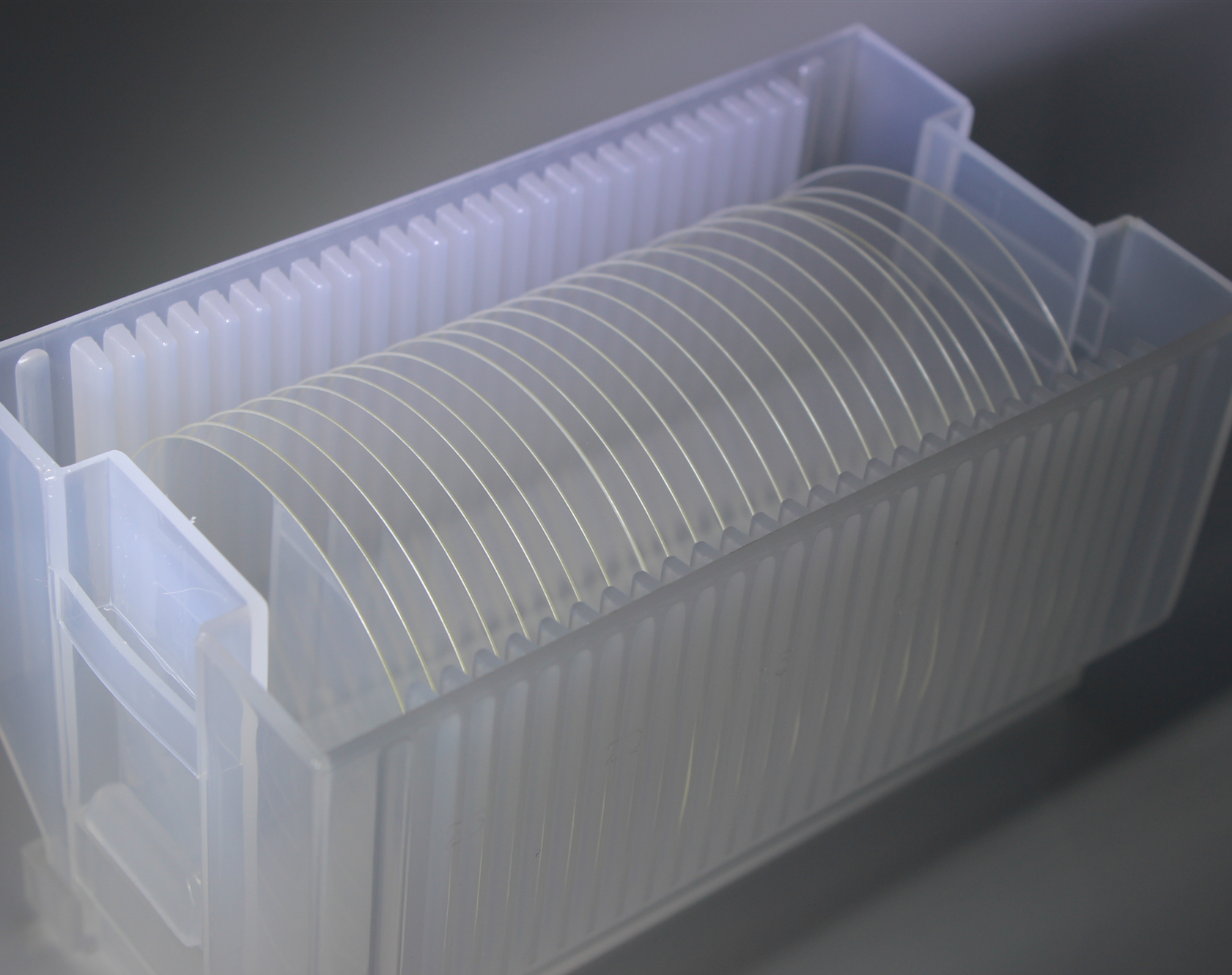
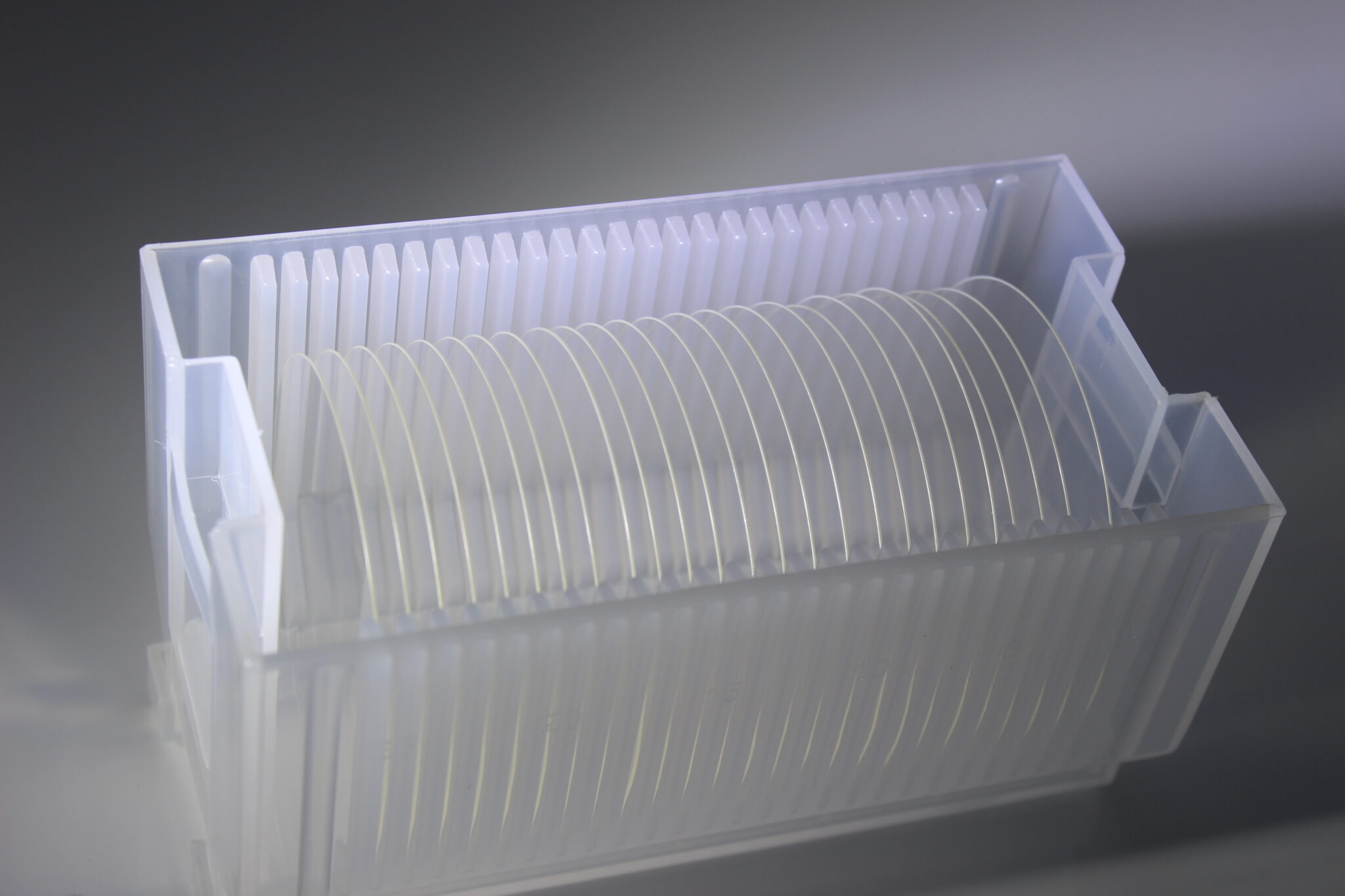
    Picture of LiNbO3 Crystal Substrates
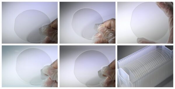
    Optical grade LiNbO3 wafer with precision polished surface

    Detailed Video of LN Wafer

    Key Features of Lithium Niobate Wafers

    • Excellent electro optical properties
    • Strong piezoelectric performance
    • High optical transparency
    • Stable crystal structure

    Applications of LiNbO3 Crystal Wafers

    • Optical modulators
    • Integrated photonic devices
    • Laser and nonlinear optical systems
    • SAW and acoustic wave devices
    • Telecommunication equipment

    Advantages of Precision Lithium Niobate Substrates

    • High electro optical efficiency
    • Reliable optical and electrical performance
    • Excellent surface quality

    People Also Ask (FAQs)

    What is LiNbO3 used for?

    LiNbO3 is widely used in optical modulators,
    photonic devices, piezoelectric components, and laser systems.

    Why is lithium niobate important in photonics?

    Lithium niobate provides excellent electro optical properties
    and is commonly used in high speed optical communication systems.

    Customization Options

    • Custom wafer diameter and thickness
    • Single side and double side polishing
    • Custom crystal orientations
    • OEM and volume production support

    Production Factory of VY Optoelectronics Co.,Ltd.

    Want to learn more / get a quote? Just click here to contact us now~

    Related Products

    ANYTHING YOU COULDN’T FIND?

    Talk With Our Sales

    Vyoptics dedicated to being the supplier you choose for your custom optic fabrication. From volume production to prototype, we will meet any require specifications at the most cost effective solution.

    • Free quotes and design consultations
    • Comprehensive brochure you can download
    • Worry-free returns
    • Lightning Delivery
    • OEM&ODM
    • Fast Respond Or enthusiasm
    • Rapid Production
    • Low MQQ

    SEND US AN EMAIL

    [email protected]

    Contact Us

    Welcome to discuss your purchasing requirements with our customer service.